HS-3a
32 BIT I/0 for
ZX to ZX Communication
Rev a - August 14, 2005 - wilf
rigter
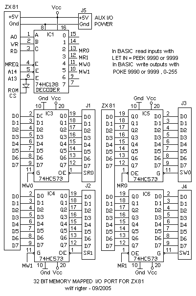
A 32 BIT MEMORY MAPPED I/O PORT FOR
THE ZX81
A
general purpose 32 bit memory mapped I/O design is presented in this
article
based on 5 simple TTL chips. A 74HC138 decoder is used to decode four
read
and write signals for reading and writing four 74HC573 OCTAL LATCHES
which
are decoded (with many echoes) in the 8K to 16K area of the memory map.
The ROM
echo normally present in this location is suppressed by connecting A13
through
a diode to the ROMCS line.
These 4
I/O ports are accessible to a BASIC program using PEEK and POKE to
any ODD
and EVEN address in this memory space.
Address 9990 and 9999 are
used by
default conveniently located on the keyboard. A FOR-NEXT loop using
N=8192
TO 16383 will access alternate ports for even and odd values of N.
Memory
mapped I/O that is accessible in alternate memory locations can also
be an
advantage in Machine Code using LDI to move a block of memory to and
from
the data input and output ports with handshaking or to simply transfer
data
from an input port to output port using handshaking.
This
interface is ideal to transfer data between a TS1000 and printer
or for
high speed communication with a PC through a printer port or for
ZX
control of a robot.
The
HS-3 is a special design application of this memory mapped I/O port for
high
speed data transfer between two TS1000 units connected back to back .

HS-3 – INTRODUCTION
The
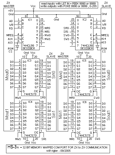
HS-3 design is a straight adaptation of the 32 BIT memory mapped I/O
circuit
using a separate 74HC138 decoder for each TS1000. Four 74HC573 octal
latches
are used for the 32 bit COM PORT. Two OUTPUT PORTS of the MASTER
TS1000
correspond directly with two INPUT PORTS of the SLAVE TS1000 and vice
versa.
The six
chip HS-3 circuit can be mounted on a PCB plugged into the MASTER
TS1000
with a single 16 conductor flex cable to connect to the SLAVE TS1000.
The
HS-3 system described here is a high speed interface for byte wide
parallel
communications between two ZX81 or TS1000 units.
In this
application, a 32 but memory mapped I/O circuit is used to connect
two
TS1000s one of which (so called SLAVE) is dedicated to executing a user
program
in an accelerated SLOW mode that replaces the ROM video routine
with a
DFILE transfer routine while the other (so-called MASTER) generates
a
continuous video display of the transferred user program DFILE.
Compare
this to the HS-2 system in which the video of a SLOW mode MASTER
TS1000
displays the DFILE of the SLAVE TS1000 using BUSRQ for direct access
to the
memory of a SLAVE TS1000 which runs the user program in the FAST
mode
using the normal ROM routines.
SLAVE TS1000 - ACCELERATED SLOW
MODE
A TS1000
in the FAST mode can run user programs full speed while the video
circuit
is turned off so no video is displayed until the user program pauses.
In the
accelerated SLOW mode, the SLAVE TS1000 video is controlled by NOVA,
the
multitasking variable video routine that transparently transfers the SLAVE
DFILE
to the HS-3 COMPORT and can generate a single line of video display for
local
STATUS and KEY INPUT. This leaves many blank video lines for the user
program
to execute at about 80%(60Hz) of the FAST mode speed.
MASTER TS1000 – SLOW MODE
The
MASTER TS1000 spends 80% of its CPU time on generating the video display
and
runs the DFILE transfer program only 20% of the CPU time during each
video
frame when video is blanked between displays.
When
the MASTER DFILE user program is running, it sets the READY bit and
then
continuously transfer the SLAVE DFILE data from the COM PORT to the
MASTER
DFILE. NMI interrupts this transfer every 64us so the MASTER and
SLAVE
use handshaking to indicate when each byte is ready.

HS-3 – DATA TRANSFER PROTOCOL
In the
HS-3 interface, the four INPUT and OUTPUT PORTS are connected
back to
back as a high speed COMMUNICATION PORT.
The
ports are designated as follows:
MASTER
OUTPUT PORTS - Mout0 and Mout1
MASTER INPUT
PORTS - Min0 and Min1
SLAVE
OUTPUT PORTS - Sout0 and Sout1
SLAVE
INPUT PORTS - Sin0 and Sin1
Protocol
uses handshaking to transfer the DFILE of the SLAVE TS1000
to the
MASTER DFILE through the memory mapped 32 bit COMPORT.
This is
not quite as fast as using a true DUAL PORTED RAM but uses
much
simpler hardware.
The
MASTER TS1000 provides a SLOW mode video display of the application
program
running in the accelerated SLOW mode on the SLAVE TS1000.
The
SLAVE uses Mout0 to write DFILE DATA, Mout1 to write the SLAVE
CONTROL
byte and Sin0 to read the MASTER control bits. The MASTER
uses
Min0 to read SLAVE DFILE data , Min1 to read the SLAVE
control
bits and Mout0 to write the MASTER control bits.
The
PORT name uses the suffix 0 or 1 to indicate if an EVEN or ODD
address
in the range 2000h to 3FFFh (8192d-16383d) controls that PORT.
The
SLAVE DFILE transfer program transfers one byte from DFILE to the
COMPORT
as follows:
1) The
DFILE starting address is loaded from (DFILE) to HL
2) The
length OF DFILE (793d) is stored in BC
3) The
16 bit PORT address (2000h) is set up in DE
4) The
MASTER BUSY bit is tested every NMI to see if the MASTER has
finished generating the video display and
is ready for data transfer
5) When
BUSY goes LOW, the MASTER RDY (MRDY) bit is tested with the
SLAVE RDY (SRDY) bit.
5) When
MRDY and SRDY are different, the SLAVE transfers a byte from
DFILE to Mout0 using the LDI instruction.
6) Then
the SRDY bit in Mout1 is set to the same state as the MRDY bit.
7) DE
is decremented or incremented as required to point to either PORT.
The
MASTER uses Min0 to read DFILE DATA, Min1 to read the SLAVE
SRDY
bit and MOUT0 to write the MASTER BUSY and MRDY bits.
The
MASTER transfer protocol is similar and transfers one byte from the
COMPORT
to DFILE as follows:
1) The
DFILE starting address is loaded from (DFILE) to DE
2) The
length OF DFILE (793d) is stored in BC
3) The
16 bit PORT address (2000h) is set up in HL
4) The
MASTER RDY (MRDY) bit is compared to the SLAVE RDY (SRDY) bit.
5) When
MRDY and SRDY are same, a byte is transferred from data Min0
using the LDI instruction.
6) Then
the SRDY bit in Mout0 is set to the opposite state as the SRDY bit.
7) HL
is decremented or incremented to point to either I/O PORT.
The NMI
line interrupts the transfer program every 64us to see if it is time
to
generate another video display. If so, the MASTER writes the BUSY bit in
Mout0
and then continues to the video routine. When the master finishes
the
video routine it rests the BUSY bit to indicate the MASTER is ready for
more
DFILE
CONTROL PROGRAM
I intend to hook the transfer program into NOVA for both the MASTER and SLAVE
control programs as outlined above. NOVA is a simple multitasking routine
that intercepts the video vector in register IX and generates a variable
length video display in place of the NORMAL ZX81 video routine. The MASTER
can display 24 or 25 lines while the SLAVE only displays one line of video
NOVA is designed for just such an application as this.
The HS-3 COMPORT is fully bi-directional and can transfer other data, such as
variables required for example for “ON LINE” game playing with two players on
two TS1000 units. Other software can use this hardware for applications like
adding input devices such as a keyboard or mouse or output devices such as a LCD.
COMMENTS
Coming...
REVISION NOTES
Revision A – change HS-3 PORT designations in text and schematic AUG 14, 2005